nanoGUNE bets for non-destructive new tech for the electrical characterization of advanced materials
Client: nanoGUNE
Description:
The CIC (Cooperative Research Center) nanoGUNE is a research center created in 2009 with the mission to address basic and applied research of the first level in nanoscience and nanotechnology, promoting the education and training of high-level researchers in this field. NanoGUNE is the first Spanish technology center to have das-Nano ONYX system. Graphenea: nanoGUNE’s first start-up, dedicated to industrial graphene manufacturing, uses Onyx technology to characterise its graphene in materials development processes.CIC nanoGUNE:
113 employees, technologically and geographically diversified.
Expertise: nanotechnology, nanoscience, nanomagnetism, self-assembly, nanobiomechanics, nanodevices, nanoimaging, nanomaterials, nanooptics and theory
Table of contents
Challenge: Mapping the electrical properties of bulk materials, thin films, and 2D materials such as graphene with high resolution, non-destructively, quickly, and without contact
What nanoGUNE needed was a fast system to inspect materials of different nature without destroying them and with high precision.
On the other hand, Graphenea wanted to inspect materials for quality control of the graphene manufacturing process and the development of new advanced materials.
Both were looking for a solution that mapped the electrical properties (such as conductance, resistance, or carrier mobility) of bulk materials, thin films, and 2D materials such as graphene with high resolution and in a non-contact, non-destructive, and fast manner.
Current methods are very slow because they are at the nanoscale (Raman, AFM, SEM, TEM) or have low resolution (DC conductivity, optical examination).
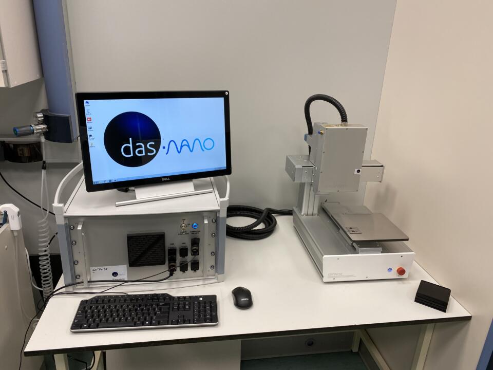
das-Nano solution: Patented technology for the non-destructive and non-contact electrical characterization of advanced materials
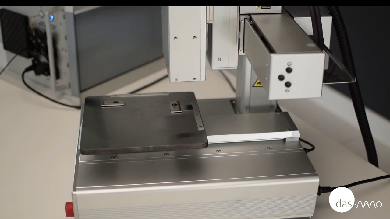
das-Nano Onyx system was the perfect solution for nanoGUNE and Graphenea. It is the first system in the market designed to provide a non-destructive and non-contact full-area characterization of graphene, thin films, and other 2D materials.
Onyx, a patented system based on terahertz spectroscopy, bridges the gap between macro- and nanoscale tools by characterising from 0.5 mm² to large areas (m²), in a non-destructive and non-contact manner, enhancing the industrialization of research materials. This technology is harmless, requires no sample preparation, and allows measuring the spatial distribution of sample quality. Spatial resolution in the order of a few hundred microns and fast acquisition and processing of terahertz signals allows rapid characterization of large sample areas.
Onyx complies with the IEC TS 62607-6-10:2021 technical specification, which deals with the measurement of the sheet resistance of graphene-based materials using terahertz time-domain spectroscopy.
In a single measurement, the system is able to provide the following physical properties:
Result: A fast and reliable tool to boost your research materials
das-Nano Onyx offers a non-destructive, non-contact, fast, and high-resolution inspection method to map electrical properties of bulk materials, thin films, and 2D materials such as graphene.
As a non-contact, non-destructive method that requires no sample preparation, unique research samples can be analysed several times with terahertz time-domain spectroscopy (THz-TDS) without modifying them.
Obtaining maps of the whole area of samples and not single points allows identification of defects, degree of homogeneity, etc.
Several scientific articles in high impact factor peer-reviewed journals have been published with data obtained with the Onyx system. The following examples have been published in collaboration with Graphenea.
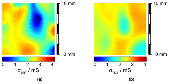
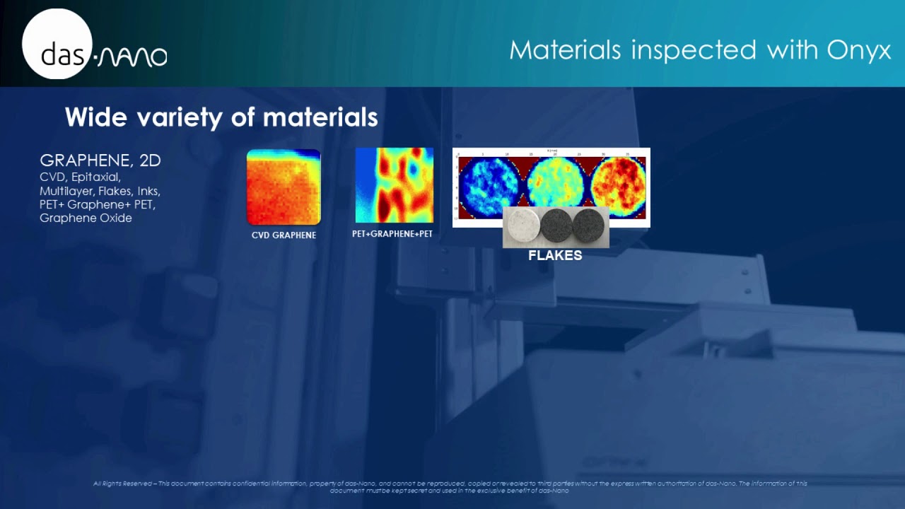
In the article “Mapping the conductivity of graphene with Electrical Resistance Tomography” (Cultrera et al, Scientific Reports, 2019, 9:10655) electrical resistance measurements on large-area graphene samples were obtained with contact methods (electrical resistance tomography (ERC) and van der Pauw measurements) and non-contact THz-TDS Onyx measurements. The chemical vapour deposited (CVD) graphene conductivity maps of 10×10 mm2 areas obtained with ERC and Onyx (TDS) are compared in the figure below. The Onyx image contains 100×100 pixels, each one corresponding to one measurement and allows identifying heterogeneities along the graphene sample surface in a non-destructive way and without contact, ensuring the integrity of the sample after the measurement.
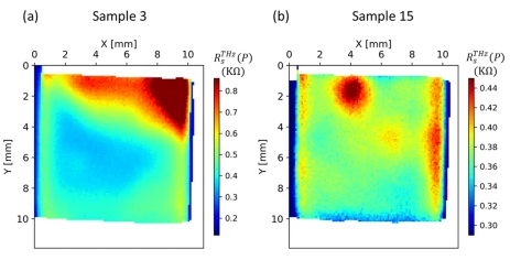
In the article “Towards standardisation of contact and contactless electrical measurements of CVD graphene at the macro-, micro- and nano-scale” (Melios et al, Scientific Reports, 2020, 10:3223) a comprehensive methodology for measurements of the electrical properties of graphene that ranges from nano- to macro- scales was demonstrated. The electrical characterisation was achieved by using a combination of techniques, including magneto-transport in the van der Pauw geometry, terahertz time-domain spectroscopy mapping with the Onyx system (two resistivity maps are shown below) and calibrated Kelvin probe force microscopy. The results exhibit excellent agreement between the different techniques.
Furthermore, two Good Practice Guides on the electrical characterization of graphene were published within the GRACE EMPIR/EURAMET project: