- IHP
IHP has the first system on the market for fast and reliable wafer quality control without material damage
Innovations for High Performance (IHP), is one of the world’s leading research institutions in the field of silicon/germanium electronics. It has extensive experience in semiconductor technology, materials research, high-frequency circuit design, and system solutions. Its technologies and electronic circuits are among the most powerful in the world.
- Industry: research and development in the field of microelectronics and information technology
- Headquarters: Frankfurt (Oder), Germany
- Employees: + 350 employees worldwide
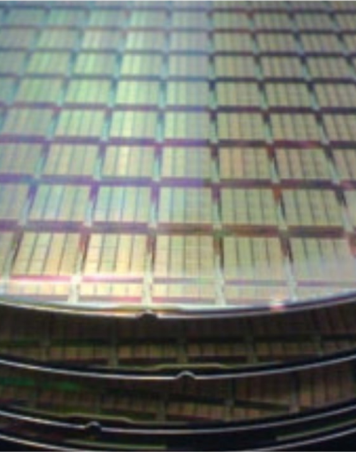
The challenge: how to measure wafers for use in microelectronics fabrication faster, more reliably and without contact
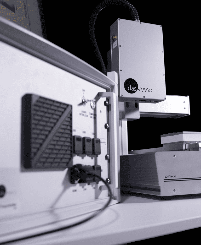
- The das-nano solution
The das-Nano solution: Patented technology for non-destructive wafer measurement process
das-Nano’s product Onyx was the perfect solution to IHP’s problem. Onyx is the first system in the market designed to provide non-destructive and non-contact full-area characterization of graphene, thin films and other 2D materials.
Onyx, a patented system based on terahertz spectroscopy, bridges the gap between macro-and nanoscale tools by characterizing from 0.5 mm² to large areas (m² ), enhancing the industrialization of research materials. This technology is harmless, requires no sample preparation and allows measuring the spatial distribution of sample quality. Spatial resolution in the order of a few hundred microns allows rapid characterization of large sample areas instead of microscopic methods.
In a single measurement, the system is able to provide the following physical properties:
- Electrical conductivity
- Electrical resistivity
- Charge carrier mobility
- Charge carrier density
- Refractive index
- Substrate thickness
The results: fast and reliable wafer quality control with no material damage
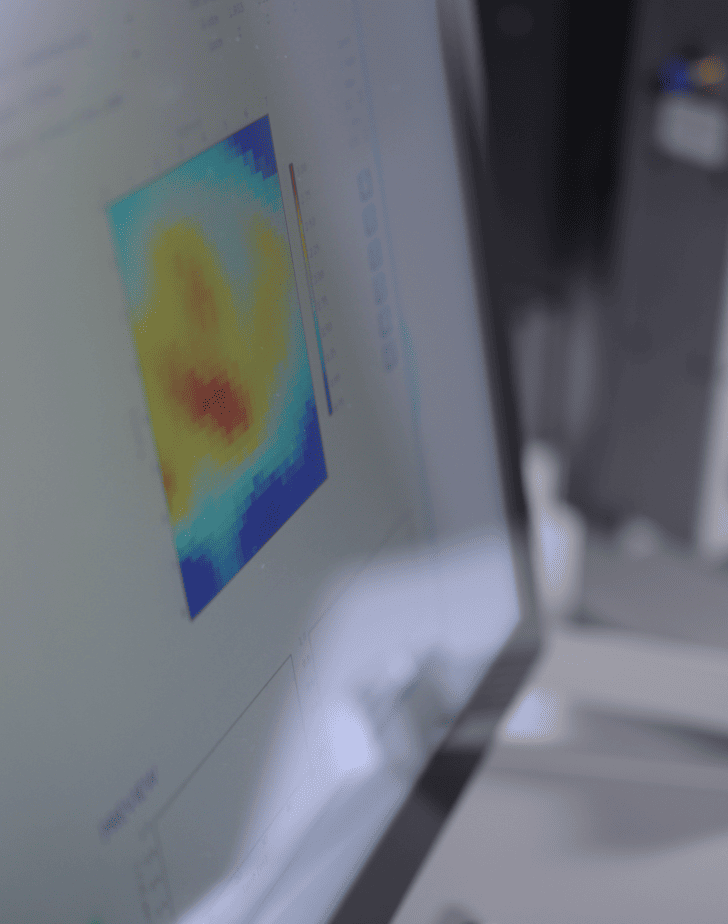
As a result, Onyx offers a nondestructive, contactless, fast and more reliable quality control process for wafers of advanced nanomaterials to be integrated into microelectronic components. Being non-destructive, each part can be analyzed individually, more reliably and efficiently. By mapping the entire wafer area rather than individual points, it allows defective parts to be identified at the earliest stage of the production process.
A more reliable and lower cost blade coating control is achieved by implementing terahertz waves in the quality control of the blades manufacturing. Thanks to the particular properties of this specific frequency of the electromagnetic spectrum, this state-of-the-art non-destructive inspection method is now commercially available.
A more reliable and lower cost blade coating control is achieved by implementing terahertz waves in the quality control of the blades manufacturing. Thanks to the particular properties of this specific frequency of the electromagnetic spectrum, this state-of-the-art non-destructive inspection method is now commercially available.
Siemens-Gamesa has relied on the NOTUS system since 2017 for the blade coating manufacturing quality control. Thanks to this technology, Siemens-Gamesa can have real-time data on the condition of its blade coatings, both during production and throughout their useful life. NOTUS is a portable device that can be used not only in the manufacturing plant, but it can also be taken to logistic hubs and wind farms to perform measurements for preventive or corrective maintenance.