- Electrical Characterization
Unlocking material performance with Terahertz Technology
The new standard in material analysis – it’s here
In industries where material performance is critical—such as batteries, semiconductors, and advanced materials like graphene and 2D materials—having precise control over electrical properties is essential. Traditional characterization methods rely on contact-based or destructive techniques, limiting their efficiency, accuracy, and scalability.

Non-destructive, contactless, and highly precise electrical property measurement
At das-Nano, we bring a new paradigm to electrical material characterization with our terahertz-based, non-contact technology. For the first time, manufacturers and researchers can measure the electrical properties of materials over large areas, without damaging or altering the sample.
- Looking for a contactless solution to assess conductivity, carrier mobility, and other key properties?
- Need to map the electrical performance of your materials with high spatial resolution?
- Want a scalable method that bridges the gap between lab research and industrial production?
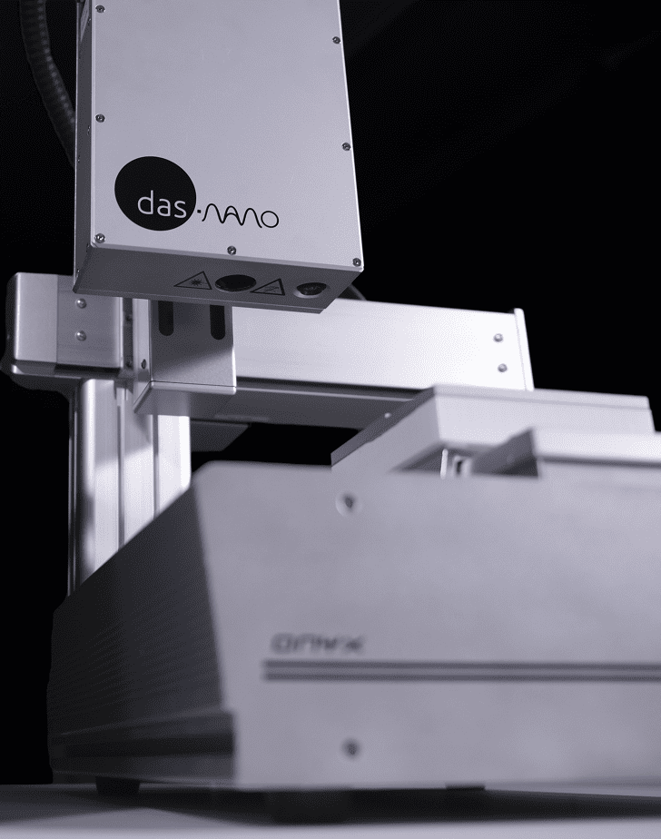
Discover ONYX
Why electrical characterization matters
In industries such as energy storage, electronics, and advanced materials, electrical properties define product performance, reliability, and efficiency. However, traditional inspection methods present key challenges:
- Graphene & 2D materials
Quality varies across a single sample, making full-area mapping critical. - Battery components
Conductivity and material uniformity directly impact energy efficiency and lifespan. - Semiconductors
Variations in electrical properties affect device performance and yield rates.
Our solution enables full-area electrical property measurement, providing a high-resolution map of conductivity, mobility, and resistivity—without the need for physical contact or sample preparation.

Beyond conventional measurement
Unlike conventional techniques like four-probe methods, Raman spectroscopy, or SEM, das-Nano’s terahertz-based solution offers:
- Non-contact measurement
No risk of sample contamination or damage. - Full-area characterization
Rapidly scan from small (0.5 mm²) to large areas (m²).
- High spatial resolution
Up to 50 µm, capturing fine variations in electrical properties. - Ultra-fast processing
Characterize entire surfaces at 12 cm²/min. - Versatility
Ideal for both industrial applications and research environments.
- Bridging R&D and industry
From research to industry: scalable, automated, and ready for production
Ready to experience the next generation of electrical material characterization?
They already trust us
- Let’s Talk
Bring precision to your material characterization
Understanding and controlling the electrical properties of materials is no longer a challenge—it’s an opportunity. Whether you’re in battery manufacturing, semiconductor development, or graphene research, das-Nano provides the cutting-edge technology you need to ensure precision, reliability, and efficiency.
- Get in touch with our experts today to explore how our non-contact, terahertz–based solution can elevate your quality control and material analysis.