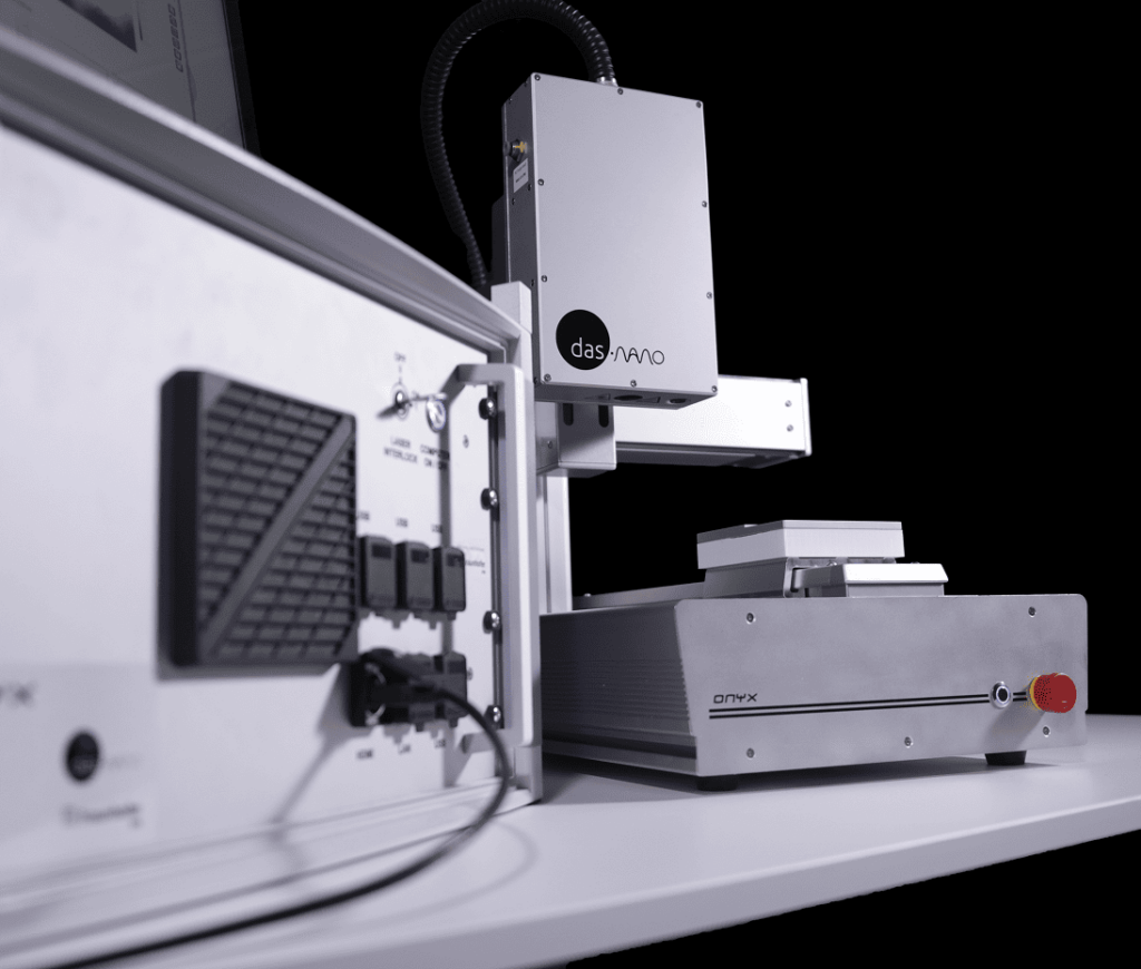
- Onyx
Experience the next era of material characterization today
Unlock new possibilities in analysis with terahertz precision
The first system of its kind, Onyx delivers full-area, non-destructive electrical characterization of graphene, thin films, and other 2D materials.
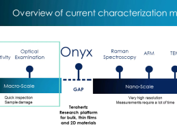
Bridging the gap between macro and nanoscale tools, it enables measurements from 0.5 mm² to entire square meters, accelerating the transition from research to industrial application.
Using THz waves technology…

To bridge the gap between macroscale and nanoscale quality inspection systems


Onyx: Precision that drives material innovation
From R&D to production, Onyx’s adaptable technology is the go-to solution for industries pushing the boundaries of material science.
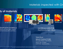
Onyx offers unparalleled material characterization across multiple industries. Whether you’re working with photovoltaics, semiconductors, smart materials, or advanced coatings, Onyx delivers precise, real-time insights that drive innovation and elevate performance.
Maximize the efficiency of thin-film coatings with advanced, non-destructive analysis.
Achieve accurate electrical property measurements to optimize semiconductor manufacturing.
Unlock the potential of dynamic materials with comprehensive, depth-related data.
Empower breakthrough research with high-precision electrical property insights.
Fine-tune components with Onyx’s advanced measurement capabilities.
Ensure consistent quality and high performance with accurate, fast, and non-invasive testing.
Watch Onyx in action!
Unlike infrared radiation, which has limited penetration capabilities, our technology uses terahertz waves that can penetrate deeper into materials, providing a more thorough analysis.
Additionally, while microwaves offer good resolution for certain applications, our solution delivers significantly higher resolution, enabling more precise measurements at a sub-millimeter level.
This combination of greater penetration and superior resolution ensures a more comprehensive understanding of material properties, making it ideal for complex material characterization.
Real-world impact: success stories from industry leaders
- DOWNLOAD ONYX TECHNICAL SHEET
Tech specifications
Discover the full capabilities of Onyx with our detailed technical sheet. Explore key specifications, performance metrics, and unique features that make Onyx the ultimate solution for advanced material characterization. Download now to see how Onyx can elevate your research and production processes
Patented and certified innovation
das-Nano holds 19 patents across key technological fields, including terahertz technology, artificial intelligence, and nanotechnology. Among them, 12 patents specifically protect groundbreaking advancements in terahertz technology.
The Onyx system complies with IEC TS 62607-6-10:2021, the technical specification established by the International Electrotechnical Commission (IEC) for measuring sheet resistance in graphene-based materials using terahertz time-domain spectroscopy.
Precision, speed, and versatility in material characterization
More accurate measurement of electrical properties
Achieve precise, reliable electrical characterization using advanced terahertz technology.
Contactless & non-destructive
Gain detailed insights without altering or damaging your materials, ensuring safe, reliable measurements every time.
Faster development of new materials
Accelerate material innovation with rapid, non-destructive testing, enabling quicker iterations and faster time-to-market.
Plug & play system
Seamlessly integrates into your existing workflow, allowing you to start testing with minimal setup time.
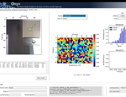
Complete visibility of your material’s electrical quality
Gain full insight into the electrical properties across the entire surface of your materials, ensuring consistency and high quality.
Full traceability of measured samples
Detailed reports and full traceability are provided for every sample, supporting better documentation and quality control.
100% inspected production
Achieve complete, contactless inspection of your production line, eliminating contamination risks and enhancing product quality.
Cost savings: early detection of production errors
Identify and address errors early in the production process to prevent costly defects, reworks, and material waste.
Optimization of electrical characterization
Maximize the effectiveness of your electrical characterization, fine-tuning material properties to enhance performance.
Reduction of defective pieces
Precise measurements help reduce defective pieces, saving costs and improving overall product quality.
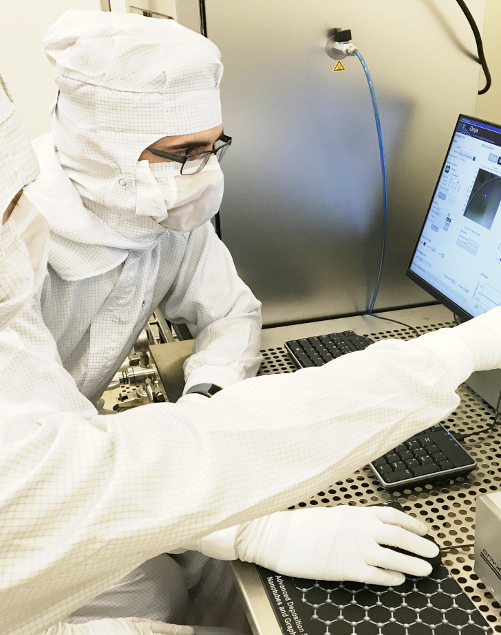
Technology for industrial manufacturing & R&D labs
Built to meet the demands of both high-volume industrial manufacturing and advanced research labs, offering flexibility and reliability.
Non-destructive electrical and structural analysis with terahertz technology
- Good spatial resolution (sub-mm): Fine resolution down to sub-millimeter precision, detecting even the smallest variations in electrical properties.
- Good penetration (~cm): Terahertz waves penetrate a few centimeters into materials, providing insights into internal properties and structures, ideal for multilayered or coated materials.
- Time-domain (depth information): Time-domain terahertz spectroscopy gathers valuable depth-related information, such as thickness and layer characterization, for a comprehensive view.
- Non-ionizing: harmless for humans: Unlike ionizing radiation technologies, it uses safe, non-ionizing terahertz waves, ensuring safety for both operators and the environment.
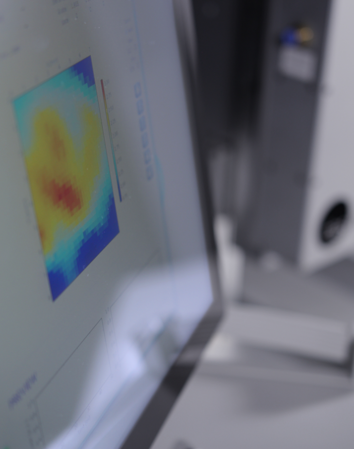
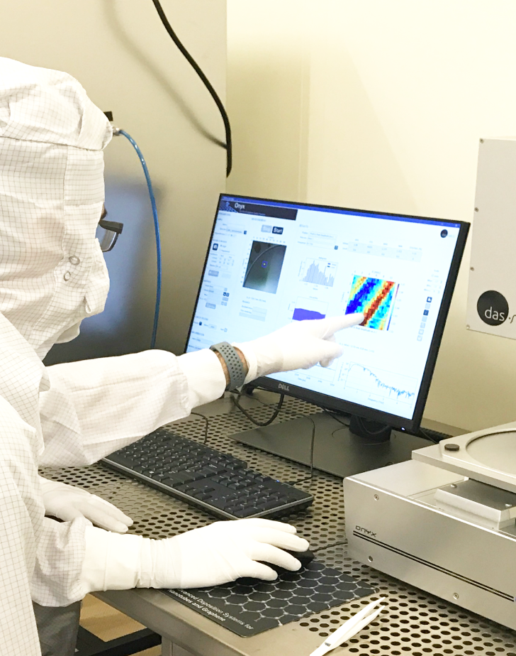
Key physical properties measured in a single scan
Unlock deep insights into your materials with the Onyx system, which provides precise measurements of essential electrical and optical properties in a single scan. These include:
- Sheet Conductance
- Sheet Resistance
- Charge Carrier Mobility
- Charge Carrier Density
- Refractive Index
- Dielectric Parameters (ε’ and ε’’)
- Absorbed Powe
- Single Frequency Features
Performance highlights
Onyx ensures high performance with the following features make it ideal for high-speed production environments and research labs:
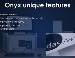
- Ultra-Fast Measurement: Up to 12 cm²/min
- High Resolution: Down to 50 µm
- Minimum Measurement Time: Just 25 ms
- Optical Camera: Ensures traceability
- Reflection Mode Measurement: Single-side inspection
Discover the wide range of material Onyx have measured
- Quartz
- Glass
- Mica
- Soda
- Lime
- Silicon (Si)
- Boron doped silicon
- Silicon carbide (SiC)
- Niobium carbide (NbC)
- 4H-SiC polytype
- Silicon oxide (SiO2)
- Magnesium oxide (MgO)
- Sapphire
- Cellulose
- Paper
- Polymers
- Porous polymers
- Transition metal dichalcogenides (TMD)
- MoS2
- WS2
- Graphene
- Layers
- Flakes
- Coated with polymers
- Graphene oxide
- Graphite paper
- Graphite cellulose nanofibers
- Carbonized lignin fibers
- Carbon nanotubes
- PEDOT:PSS
- Polymers
- Hexagonal boron nitride (h-BN) and hBN C doped
- Copper (Cu)
- Nickel (Ni)
- Silver (Ag)
- Aluminum (Al)
- Platinum (Pt)
- Ruthenium (Ru)
- Germanium (Ge)
- Antimony (Sb)
- Gallium (Ga)
- Tungsten (W)
- InGaZnO
- Titanium oxide (TiO2)
- Niobium doped TiO2
- Indium tin oxide (ITO)
- Gallium nitride (GaN)
- Titanium nitride (TiN)
- Silver-nanowires (Ag)
- Yttrium barium copper oxide (YBCO)
Onyx Academy: the playlist
- Onyx in the GRACE Project
Developing electrical characterization methods for future graphene electronics
das-Nano collaborated on the GRACE EUROPEAN Project (EMPIR-EURAMET program), developing electrical characterization methods for future graphene electronics, such as Terahertz technology used by the Onyx device.
A Good Practice Guide on the Electrical characterisation of graphene using non-contact and high-throughput methods was published within the project.