CIEMAT trusts on patented tech for non-destructive electrical characterization in photovoltaic applications
Client: CIEMAT
Description:
CIEMAT (Centro de Investigaciones Energéticas, Medioambientales y Tecnológicas) is a Public Research Organization attached to the Spanish Ministry of Science and Innovation, mainly focused on the scientific fields of energy and the environment and the technologies related to both. CIEMAT’s mission is to contribute to the sustainable development of Spain and the quality of life of its citizens through the generation and application of scientific and technological knowledge.
1,328 employees, technologically and geographically diversified.
Headquarters: Madrid, Spain
Expertise: science, research, energy, environment and technology.
Table of contents
The challenge: Mapping the electrical properties of devices for photovoltaic applications with high resolution, non-destructively, quickly, and without contact
Current mapping methods for electrical characterization are very slow because they are at the nanoscale (Raman, AFM, SEM, TEM) or have low resolution (DC conductance, optical scanning). Cutting-edge research materials can be very difficult to fabricate, therefore, non-contact and non-destructive inspection methods are very useful to gain deeper knowledge and advance faster in cutting-edge research.
CIEMAT was looking for a solution that mapped the electrical properties (such as conductance, resistance, carrier mobility) of devices for photovoltaic applications with high resolution and in a non-contact, non-destructive and fast manner.
For photovoltaic device manufacturing, non-destructive testing (NDT) makes it possible to inspect each device and detect any defects at the earliest possible stage.
das-Nano solution: Patented technology for the non-destructive and non-contact electrical characterization of photovoltaic devices
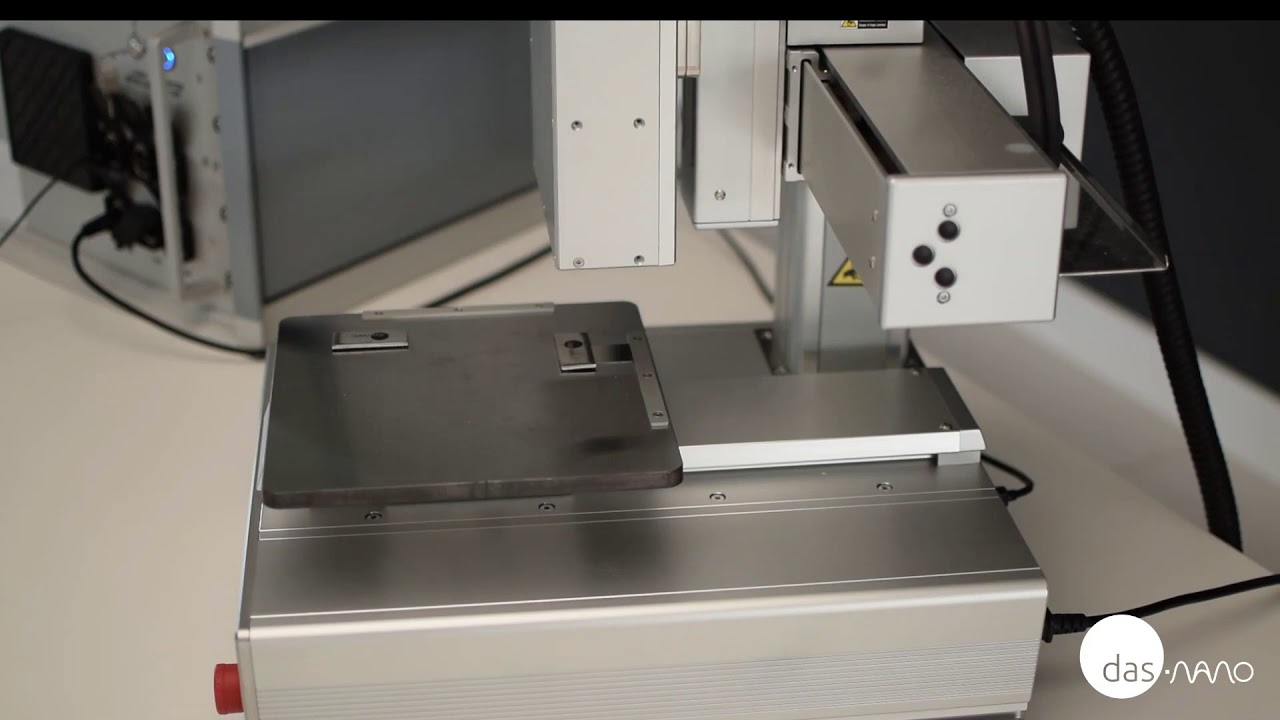
das-NanoOnyx system was the perfect solution forCIEMAT. It is the first system in the market designed to provide a non-destructive and non-contact full-area characterization of graphene, thin films, and other 2D materials.
Onyx, a patented system based onterahertz spectroscopy, bridges the gap between macro-and nanoscale tools by characterizing from 0.5 mm²to large areas (m²), in a non-destructive and non-contact manner, enhancing the industrialization of research materials. This technology is harmless, requires no sample preparation, and allows measuring the spatial distribution of sample quality. Spatial resolution in the order of a few hundred microns and fast acquisition and processing of terahertz signals allows rapid characterization of large sample areas.
Terahertz (THz) waves are low-energy, non-ionizing waves and therefore harmless to humans.
Onyx complies with theIEC TS 62607-6-10:2021 technical specification. IEC TS 62607-6-10:2021 deals with the measurement of the sheet resistance of graphene-based materials using terahertz time-domain spectroscopy.
In a single measurement, the system is able to provide the following physical properties:
Result: A fast and reliable quality control process
das-Nano Onyx offers a non-destructive, non-contact, fast, and reliable quality control process for mapping the electrical properties of devices for photovoltaic applications.
As a non-contact, non-destructive method that requires no sample preparation, unique research samples can be analyzed several times with terahertz time-domain spectroscopy (THz-TDS) without modifying them. In addition, quality control of the photovoltaic device manufacturing process can be significantly improved, as each device can be inspected without being damaged or modified, allowing early detection of defects.
Obtaining maps of the entire area of the samples rather than individual points allows identification of defects, degree of homogeneity, etc.
In collaboration with CIEMAT, das-Nano has co-authored several scientific peer-reviewed articles focused on conductive electrodes for photovoltaic applications and electrodes for silicon hetero junction solar cell technology.
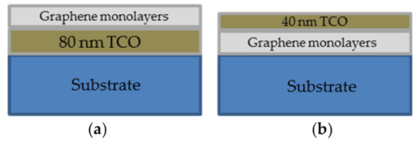
In the article “Advanced Graphene-Based Transparent Conductive Electrodes for Photovoltaic Applications” (Fernández et al, Micromachines 2019, 10, 402) new architectures of transparent conductive electrodes (TCEs) incorporating graphene monolayers in different configurations were explored with the aim to improve the performance of silicon-heterojunction (SHJ) cell front transparent contacts
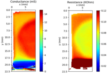
Onyx system was used to map the electrical conductance and resistance of the electrodes (see Figure 2), without the need for any sample preparation. An average conductance value of 13.12 mS was obtained for the optimum hybrid indium tin oxide (ITO)-based TCE deposited on silicon (Si) substrate, which is very promising since it is higher than the ITO value (> 10 mS).
Figure 2. Conductance and resistance maps of the optimum hybrid indium tin oxide (ITO)-based TCE deposited on silicon (Si) substrate.
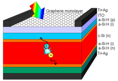
In the article “Transparent electrodes based on graphene” (Fernández et al., Nanotechnol Adv Mater Sci, Volume 2(3): 1–3, 2019) novel architectures of transparent electrodes incorporating graphene into its design are explored to improve the silicon-heterojunction-cell technology.
Figure 3. Scheme of the finished silicon heterojunction solar cell.
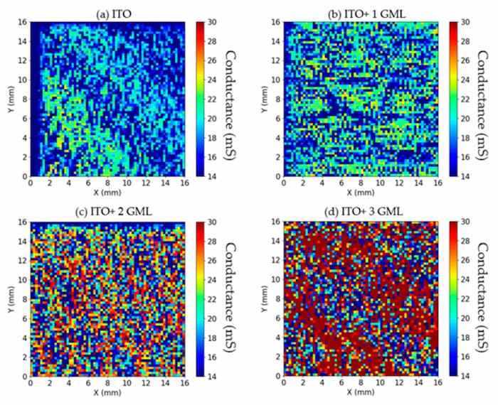
In the article “Graphene-Based Electrodes for Silicon Heterojunction Solar Cell Technology” (Torres et al., Materials 2021, 14, 4833) the effect of combining indium tin oxide (ITO) with between one and three graphene monolayers as the top electrode in silicon hetero junction solar cells was analyzed.
Figure 4 shows the maps of the conductance obtained with the Onyx system for the cells with indium tin oxide (ITO) (a), with ITO + 1 (b), ITO + 2 (c) and ITO + 3 (d) graphene monolayers. The obtained conductance maps showed a clear electrical improvement with each additional graphene sheet. In the electrical characterization of the finished solar cells, this translated to a meaningful reduction in the series resistance and an increase in the device’s fill factor