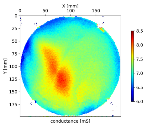
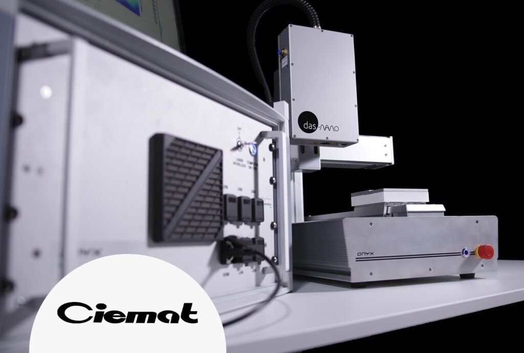
Onyx is the first system on the market designed to provide whole area non-destructive characterization of graphene, thin films, and other 2D materials. Bridges the gap between macro and nanoscale tools, characterizing from 0.5 mm² to large areas (m²), improving the industrialization of materials research.
Compared with other large-area methods, such as the four-probe method (destructive and contact), Onyx can measure the quality of the sample, providing a complete map of its surface for each electrical property being measured. Spatial resolution on the order of a few hundred microns allows rapid characterization of large sample areas, unlike microscopic methods such as Raman, SEM, and TEM.
Proprietary technology
Leading technology
System benefits
Non-contact measurement
Ultra-fast characterization of the entire surface (12cm²/min)